Advanced materials have been an aspect of this technology race adoption.
To enable the devices of today and tomorrow, manufacturers are utilizing new advanced materials. The use of high-frequency laminates, which is critical for communications and radar-based applications has widely seen an adoption. Explore additional demand information as provided by Rogers Corporation, who predicts an increase of over 20% for their high-frequency materials solutions. These materials aid both faster signal speeds as well as support the integrity of a signal in more complicated circuit designs.
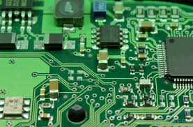
Shrinks and HDI TechnologyWidely relied on within the industry is to create ever smaller cells through standard component miniaturization, as well as High-Density Interconnect technology (HDI).
PCB Design is a field that continues to evolve with developments in technology, and miniaturisation has been pushing its limits for quite some time now. This makes use of High Density Interconnect (HDI) technology, which allows for smaller lines and spaces as well as vias and the interconnection pad densities. The HDI segment, for its part, is expected to witness an annual growth rate of as much as 12.5% according to the latest industry analysis released by Research Report Insights on Thursday; a clear indication of the high demand in increasingly smaller yet still powerful electronic devices. This growth is primarily driven by the consumer electronics and automotive sectors, where space savings and performance enhancements are critical.
Emphasis on Sustainability
Putting more sustainability measures into effect with PCB manufacturing. While environmental regulations get tighter and consumer tastes change in favour of greener products, manufacturers are tweaking their practices to follow suit. The results include making the new lead-free solders, recycling waste materials, and limiting further use of hazardous chemicals. A poll by IPC states that more than 50% of PCB manufacturer has implemented a water recycling system to reduce noxious waste.
AI and Automation Integration
PCB manufacturing with Artificial intelligence (AI) and automation is changing forever. Many production lines are now using an automated optical inspection system with AI capabilities. Traditional paradigms, on the other hand are improved as much 90% more defects can be detected with these systems. Additionally, predictive maintenance with the assistance of AI prevents downtime utilizing an equipment failure and keeps the production yield continuous.
Growth of Flexible PCBs
Flexible PCBs are being used in a number of industries. They are perfect for wearable technology, medical devices and automotive applications because of their versatility to be fit into unusual places. Also, the flexible PCB market is expected to grow 15% a year in next five years according to data by Market Research. According to the research, the rise in this market is due to the need for flexible displays and planar devices that are expecting versatile circuit solutions.
The bottom-line is, through the use of more advanced materials, IoT devices are beginning to be miniaturized with concepts like HDI technology and employed in green designs that can eliminate a total failure for workable serviceability.It also now includes automation along-side AI driven Service Mechanics. The arrival of flexible PCB into its picture allows multiple applications//*’s to bring even higher demands on consumer electronics near at hand. What these trends do is to reflect the PCB manufacturing technological advances and the industry ability or agility, if you will, in a fast-moving tech world.